|| Diagnostic Tools || Help Desk || Contribute || About || Contact || Home ||
|
|
|
|| Database Index
|| Find Manuals
|| Bios info
|| Manufacturers
|| Testing Tips || || Diagnostic Tools || Help Desk || Contribute || About || Contact || Home || |


|
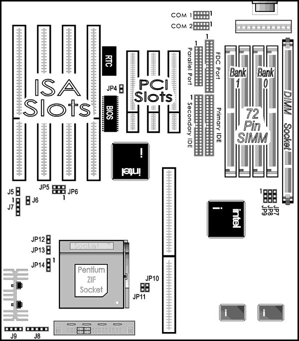
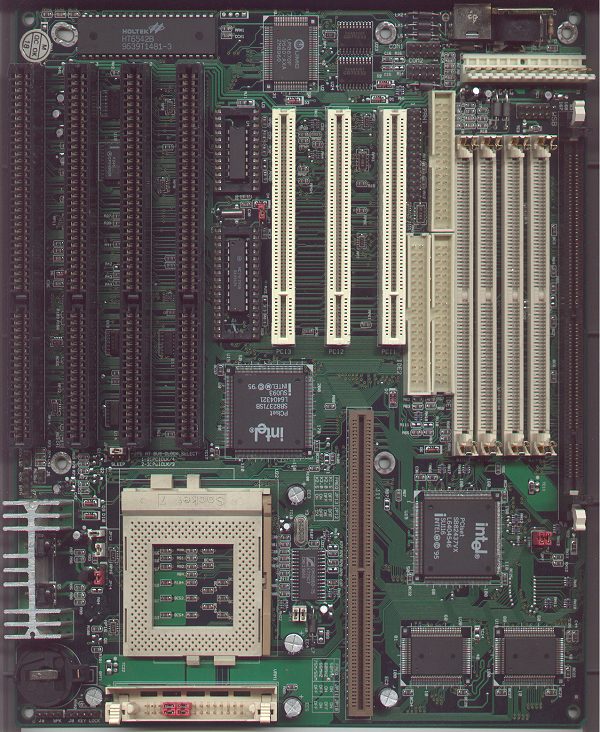
M520 v1.0 Pentium Motherboard
        - Award Bios id string   08/26/96-i430VX-2A59Ht5BC-00
        - 4-72 pin SIMM slots  (8-128MEG FPM/EDO)
        - 1-168pin DIMM slot   (8-64MEG DRAM/SDRAM/EDO)
        - 3-32bit PCI Bus slots
        - 4-16bit ISA slots
        - 160pin 256K/512K pipeline cache COAST 3.0+ module optional
        - AWARD Auto-Detect Flash Bios with Energy Mgmt.
        - Supports LBA Mode Control & Large Disk DOS Compatibility.
        - Green PC Connector
        - PS/2 Mouse Connector
        - USB connectors
        - Intel Triton PCIset SB82437VX chipset
        - DALLAS DS12887A Real Time Clock with builtin cmos battery
        - P55c Voltage Regulator Module (VRM) optional
        - Supports 3.3v/3.5v CPU's and clock speeds 1.5x/2x/2.5x/3x.
        - 321pin ZIF socket 7 which supports these processors:
          INTEL Pentium P54C-75/90/100/120/133/166/180/200 MHz, P55C w/VRM
          Cyrix/IBM 6x86 P120+/P150+/P166+, AMD K5 PR75~PR166 CPUs
        - Supports 50/60/66 MHz external clock speeds
        - Multi-I/O chip supports:
          2 PCI Enhanced IDE Ports (Supports 4 Devices PIO 0-4)
          2 High Speed Serial Ports (16550 UART Compatible)
          1 Enhanced Parallel Port (SPP, EPP, ECP capable)
          1 Floppy Drive Port (Supports 2 Floppy Drives)
        - Manufactured by: 1437 Hsing Tech Enterprise Co., LTD.
        - Sold as: Ability, Amptron, Aristo, Eurone/Matsonic, Houston Tech,
                       PCWare(Alton), Protac, PcChips, and Sybercom


======================================================================
          THIS MODEL HAS 4-16BIT ISA & 3-32BIT PCI SLOTS
======================================================================

Internal Battery                J7      2-3
External Battery                J7      closed  :-)
Clear CMOS memory               J7      3-4
Flash BIOS 5volt or EPROM       JP4     open
Flash BIOS 12volt               JP4     closed

The USB cables are optional. However, the pinout of the
internal USB cables are standardized.
                           PIN 1: VCC
                           PIN 2: Data+
                           PIN 3: Data-
                           PIN 4: GND
                           PIN 5: GND/ N.C.

The internal PS/2 mouse connector was optional.
However, the best source to find the correct PS/2
mouse cable is from your M/B or system vendor.
                           PIN 1: Data
                           PIN 2: N.C.
                           PIN 3: GND
                           PIN 4: VCC
                           PIN 5: CLK
                           PIN 6: N.C.

DIMM Voltage    JP7     JP8     JP9
------------------------------------
3.3v            2-3     2-3     2-3
5v              1-2     1-2     1-2

- Bank 0 (sockets 1&2) and DIMM cannot be used at the same time.
- All SIMMs and DIMM module speeds must be faster than 70ns.
- SIMM DRAM can be FPM (Fast Page Mode) or EDO (Extend Data Out).
- DIMM DRAM can be FPM or EDO or SDRAM (Synchronous DRAM).
- SDRAM DIMM module must be set to 3.3 volts.


CACHE Size              SL1                             TAG
----------------------------------------------------------------
256K            256K module installed           1 - 8k/16k/32kx8
512K            512K module installed           1 - 16k/32kx8

======================================================================

[ I N T E L   C O N F I G U R A T I O N ]

CPU Speed  CLOCK  Multiplier    JP5     JP10    JP11    JP12    JP13
----------------------------------------------------------------------
75MHz      50MHz    1.5x        2-3     closed  closed  open    open
90MHz      60MHz    1.5x        1-2     open    closed  open    open
100MHz     66MHz    1.5x        1-2     closed  open    open    open
120MHz     60MHz      2x        1-2     open    closed  closed  open
133MHz     66MHz      2x        1-2     closed  open    closed  open
150MHz     60MHz    2.5x        1-2     open    closed  closed  closed
166MHz     66MHz    2.5x        1-2     closed  open    closed  closed
180MHz     60MHz      3x        1-2     open    closed  open    closed
200MHz     66MHz      3x        1-2     closed  open    open    closed


[ A M D    C O N F I G U R A T I O N ]

CPU Speed  CLOCK  Multiplier    JP5     JP10    JP11    JP12    JP13
----------------------------------------------------------------------
75MHz      50MHz    1.5x        2-3     closed  closed  open    open
90MHz      60MHz    1.5x        1-2     open    closed  open    open
100MHz     66MHz    1.5x        1-2     closed  open    open    open
120MHz     60MHz    1.5x        1-2     open    closed  open    open
133MHz     66MHz    1.5x        1-2     closed  open    open    open


[ C Y R I X     C O N F I G U R A T I O N ]

CPU Speed  CLOCK  Multiplier    JP5     JP10    JP11    JP12    JP13
----------------------------------------------------------------------
120MHz     60MHz      2x        1-2     open    closed  closed  open
133MHz     66MHz      2x        1-2     closed  open    closed  open
150MHz     60MHz      2x        1-2     open    closed  closed  open
166MHz     66MHz      2x        1-2     closed  open    closed  open


CPU Voltage     JP14
---------------------
3.3 (STD/VR)    2-3
3.5 (VRE)       1-2

Do I use STD(VR) or VRE voltage?
  One of the most common questions is "Do I use STD (VR) or VRE settings
  when I replace my CPU (processor)?".
  For all Intel Pentium® CPUs - look at Pin Side (Underside) SXXXX / SMU

  If the first letter after the '/' is an 'S' the voltage is
  Standard (STD.or VR). (STD = 3.135v - 3.6v)
  If the first letter after the '/' is a 'V' the voltage is
  Voltage Regulator Enhanced (VRE).  (VRE = 3.4v-3.6v)

  For those who are interested the next letter (in this case the 'M')
  indicates the timing (M for min valid MD timings and S for min valid
  standard timings) and the last letter (the 'U' above) indicates whether
  the processor can be used with multiprocessing motherboards
  (i.e. more than one processor). If the letter is a 'U' then it has
  been tested for single processing only - if it is a 'S' then it has
  been tested for, single, dual and multi-processing.
======================================================================


======================================================================

M520 Mainboard BIOS Information:
========================================================
           Flash ROM Voltage and Block Size
  EEPROM chip    Voltage  Block Size      BIOS file
  MX28F1000PX      12 V   Large 16 K   (xxxxxxx)L.bin
  MX28F1000PL      12 V   Large 16 K   (xxxxxxx)L.bin
  MX28F1000PC      12 V   Large 16 K   (xxxxxxx)L.bin
  MX28F1000PPC     12 V   small 4 K    (xxxxxxx)s.bin
  i28F001BX-T120   12 V   small 4 K    (xxxxxxx)s.bin
  SST 29EE010      5 V    small 4 K    (xxxxxxx)s.bin
  Winbond 29EE011  5 V    small 4 K    (xxxxxxx)s.bin
  ATMEL 29C010     5 V    small 4 K    (xxxxxxx)s.bin
========================================================

awdflash.zip
     AWARD Flash Utility for upgrade of flash-BIOS

5200702l.bin checksum: * 15F3 *
     BIOS Date:07/02/1996.L FOR M525 & M520 PnP (for Block size=16K flash ROM, e.g.
     MX 28F1000PL)
     Board Description:Intel PCIset SB82437VX,SB82371SB and SB82438VX
     BIOS Features:To support IDE LBA mode(>512MB),IDE block
     mode,AUTO banking DRAM size and addition CYRIX CPU title.

5200702s.bin checksum: * DF56 *
     BIOS Date:07/02/1996.S FOR M525 & M520 PnP (for Block size=4K flash ROM, e.g. intel
     P28F001BXT, SST PH29EE010, Winbond W29EE011 )
     Board Description:Intel PCIset SB82437VX,SB82371SB and SB82438VX
     BIOS Features:To support IDE LBA mode(>512MB),IDE block
     mode,AUTO banking DRAM size and addition CYRIX CPU title.

5200831l.bin checksum: * 8122 *
     BIOS Date:08/31/1996 L. FOR M525 & M520 PnP (for Block size=16K flash ROM, e.g.
     MX 28F1000PL)
     Board Description:Intel PCIset SB82437VX,SB82371SB and SB82438VX
     BIOS Features:To support IDE LBA mode(>512MB),IDE block
     mode,AUTO banking DRAM size and addition CYRIX CPU title.

5200831s.bin checksum: * 5A18 *
     BIOS Date:08/31/1996 S. FOR M525 & M520 PnP (for Block size=4K flash ROM, e.g.
     intel P28F001BXT, SST PH29EE010, Winbond W29EE011 )
     Board Description:Intel PCIset SB82437VX,SB82371SB and SB82438VX
     BIOS Features:To support IDE LBA mode(>512MB),IDE block
     mode,AUTO banking DRAM size and addition CYRIX CPU title.

5301020l.bin checksum: * 0708 *
     BIOS Date:10/20/1996 L. FOR M530 & M525 & M520 PnP (for Block size=16K flash
     ROM, e.g. MX 28F1000PL)
     Board Description:Intel PCIset SB82437VX,SB82371SB and SB82438VX
     BIOS Features:To support IDE LBA mode(>512MB),IDE block
     mode,AUTO banking DRAM size and addition CYRIX CPU title.

5301020s.bin checksum: * A753 *
     BIOS Date:10/20/1996 S. FOR M530 & M525 & M520 PnP (for Block size=4K flash
     ROM, e.g. intel P28F001BXT, SST PH29EE010, Winbond W29EE011 )
     Board Description:Intel PCIset SB82437VX,SB82371SB and SB82438VX
     BIOS Features:To support IDE LBA mode(>512MB),IDE block
     mode,AUTO banking DRAM size and addition CYRIX CPU title.

5300303s.bin checksum: * 8835 *
     BIOS Date:03/03/1997 S. FOR M538 & M535 & M530 & M525 & M520 PnP (for Block
     size=4K flash ROM, e.g. intel P28F001BXT, SST PH29EE010, Winbond W29EE011 )
     Board Description:Intel PCIset SB82437VX,SB82371SB and SB82438VX
     BIOS Features:To support AMD K5 PR166 & K6, Cyrix M2 CPU, IDE LBA
     mode(>512MB),IDE block
     mode,AUTO banking DRAM size and addition CYRIX CPU title.

5300916l.bin checksum: * 8192 *
     BIOS Date:09/16/1997 L. FOR M538 & M535 & M530 & M525 & M520 PnP (for Block
     size=16K flash ROM, e.g. MX 28F1000PL)
     Board Description:Intel PCIset SB82437VX,SB82371SB and SB82438VX
     BIOS Features:To support IDE LBA mode(>512MB),IDE block
     mode,AUTO banking DRAM size and addition CYRIX CPU M2 title.

5300916s.bin checksum: * CBE5 *
     BIOS Date:09/16/1997 S. FOR M538 & M535 & M530 & M525 & M520 PnP (for Block
     size=4K flash ROM, e.g. intel P28F001BXT, SST PH29EE010, Winbond W29EE011 )
     Board Description:Intel PCIset SB82437VX,SB82371SB and SB82438VX
     BIOS Features:To support AMD K5 PR166 & K6, Cyrix M2 CPU, IDE LBA
     mode(>512MB),IDE block
     mode,AUTO banking DRAM size and addition CYRIX CPU M2 title.

P.S. M520 mainboard can use two types of Flash ROM __ 5 volt and 12 volt
     Set the mainborad for either type with jumper JP4.

                       12 volt flash EEPROM ====> JP4 = closed

                       5 volt flash EEPROM =====> JP4 = open

( P.S. I suggest you to burn the new BIOS file into a new EPROM
 or new Flash ROM and replace your current BIOS.(your old bios saved,
 then if cannot use new bios use the old bios chip again. Because many
 people make mistakes when update BIOS... the system cannot work again.))

=========================================================================
|
|