


| Company | Headlines | Products | Downloads | Support | Comments |
| Awards | Certificates | Employment | Search | Site Map | Home |


 Chapter set above: Mainboard HOT-419 (486, AT, OPTi)
 Configuration tables for HOT-419DZ/R2
Chapter set below:
CPUs
Systemclock
CPU voltage
VL-Bus settings
Memory
Cache size
CPUs
| Jumper | AMD 486 NV8T | Intel S-Series | Cyrix DX/DX2 |
| 3 | 1-2 | 1-2 | 1-2 |
| 5 | 2-3 | 2-3 | 2-3 |
| 8 | 1-2 | 1-2 | 1-2 |
| 42 | open | 1-2 | 2-3 |
| 43 | DX2: 1-2 | 1-2 | 2-3 |
| 44 | open | closed | open |
| 45 | open | closed | open |
| 46 | open | closed | open |
| 47 | open | open | closed |
| 48 | open | open | closed |
| 49 | 1-2 | 1-2 | 2-3 |
| 65 | . | Multiplier for DX4: | . |
| 77 | 1-2 | 2-3 | 1-2 |
| Jumper | AMD 486 SV8B | Intel 486SX | Intel 486SX |
| 3 | 1-2 | open | open |
| 5 | 2-3 | 2-3 | 2-3 |
| 8 | 1-2 | 1-2 | 1-2 |
| 42 | open | open | 1-2 |
| 43 | 1-2 | 1-2 | 1-2 |
| 44 | open | open | closed |
| 45 | open | open | closed |
| 46 | open | open | closed |
| 47 | open | open | open |
| 48 | open | open | open |
| 49 | 1-2 | 1-2 | 1-2 |
| 59 | write back: closed | . | . |
| 77 | 1-2 | . | . |
Systemclock
| Systemclock | JP22 JP21 JP23 |
| 20 MHz |
|
| 25 MHz |
|
| 25 MHz |
|
| 33 MHz |
|
| 33 MHz |
|
| 40 MHz |
|
| 50 MHz |
|
| 50 MHz |
|
CPU voltage
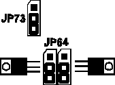
| CPU voltage | JP64 | JP73 |
| 3V |
|
|
| 3.3V |
|
|
| 3.45V |
|
|
| 5V |
| No effect |
VL-Bus settings
| VL-Bus Speed - JP34 | |
| 33 MHz or more |
|
| below 33 MHz |
|
| High Speed Write- JP33 | |
| No Waitstate |
|
| 1 Waitstate |
|
| CPU DRY# Signal Delay - JP55/69 | |
| Setup 1 |
|
| Setup 2 |
|
| Address hold time (ADS#) - JP36 | |
| Normal operation |
|
| Delay CPU ADS# signal |
|
Memory
HOT-419 provided two memory configuration modes, mode 1 and mode 2. Jumpers JP60, JP61, JP62, JP70, JP71, and JP72 are provided to configure the memory configuration between two memory configuration modes. In Mode 1 the mainboard supports 4 banks of socalled single density modules in sizes of 1, 4, 16 or 64MB. Mode 2 supports double density modules in sizes of 2, 8, or 32MB, too - but only 3 banks: the memory socket next to the ISA expansion slot must be left empty. The mainboard supports a total size of 2 to 128MB memory.
| Memory Mode 1 | Memory Mode 2 |
|
|
|
Note:
When memory configuration mode 1 is selected, HOT-419 mainboard supported two VESA master local bus slot, one on J20 (VL Bus slot 1), and the other one on J19 (VL-Bus slot 2) or J18 (VL-Bus slot 3).
If memory configuration mode 2 is selected, HOT-419 mainboard only supported one VESA master local bus slot on J18 or J19, J20 is assigned to slave always.
Cache size
| Cache | Data SRAM | Data SRAM | Tag RAM | JP 10, JP13 |
| 64 kB | 8k x 8 | 8k x 8 | 8k x 8 |
|
| 128 kB | 32k x 8 | empty | 32k x 8 |
|
| 256 kB | 32k x 8 | 32k x 8 | 32k x 8 |
|
| 512 kB | 128k x 8 | empty | 32k x 8 |
|
 © 1999 Shuttle Inc., Last modification: 01/13/2000
All other brand and product names within this page are the property of their respective owners. Shuttle assumes no responsibility for any errors or omissions. Nor does Shuttle make any commitment to update information, with or without prior notification.
