NIAGARA SMD TECHNOLOGY, INC.
NT928SPP
|
Processor |
Pentium Pro |
|
Processor Speed |
150/166/180/200/210/233/240/266/270/300MHz |
|
Chip Set |
Intel |
|
Video Chip Set |
None |
|
Maximum Onboard Memory |
512MB (EDO supported) |
|
Maximum Video Memory |
None |
|
Cache |
256/512KB (located on Pentium Pro CPU) |
|
BIOS |
AMI/Award/Phoenix |
|
Dimensions |
305mm x 244mm |
|
I/O Options |
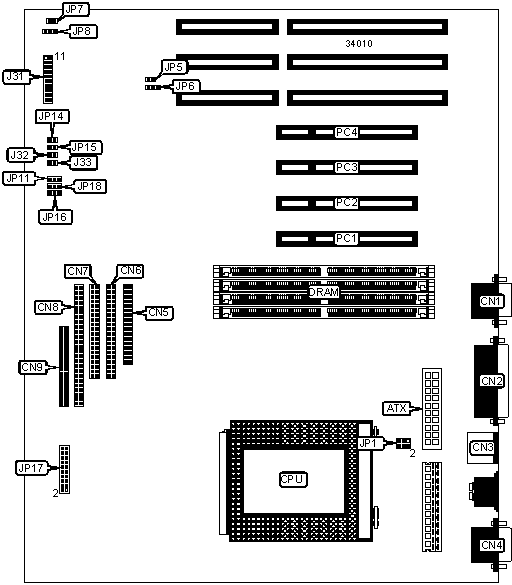
32-bit PCI slots (4), floppy drive interface, green PC connector, IDE interfaces (2), Ultra-SCSI Wide interface, SCSI interface, parallel port, PS/2 mouse port, serial ports (2), ATX power connector, USB connector, IR connector |
|
NPU Options |
None |
|
CONNECTIONS | |||
|
Purpose |
Location |
Purpose |
Location |
|
ATX power connector |
ATX |
Speaker |
J31 pins 1 - 4 |
|
Serial port |
CN1 |
Power LED & keylock |
J31 pins 6 - 10 |
|
Parallel port |
CN2 |
Reset switch |
J31 pins 11 & 12 |
|
PS/2 mouse port |
CN3 |
SCSI LED |
J31 pins 13 & 14 |
|
Serial port |
CN4 |
IDE interface LED |
J31 pins 15 & 16 |
|
Floppy drive interface |
CN5 |
Green PC connector |
J31 pins 17 & 18 |
|
IDE interface |
CN6 |
Turbo LED |
J31 pins 19 & 20 |
|
IDE interface |
CN7 |
Power on/off switch |
JP7 |
|
SCSI interface |
CN8 |
Remote power switch |
JP8 |
|
Ultra-SCSI Wide interface |
CN9 |
32-bit PCI slots |
PC1 – PC4 |
|
Note: The location of the IR &USB connectors are unidentified. | |||
|
USER CONFIGURABLE SETTINGS | |||
|
Function |
Label |
Position | |
|
» |
Factory configured - do not alter |
J32 |
Unidentified |
|
Wide SCSI enabled |
J33 |
Closed | |
|
Wide SCSI disabled |
J33 |
Open | |
|
» |
Auto power enabled |
JP5 |
Closed |
|
Auto power disabled |
JP5 |
Open | |
|
» |
Factory configured - do not alter |
JP6 |
Unidentified |
|
SCSI chip enabled |
JP11 |
Pins 1 & 2 closed | |
|
SCSI chip disabled |
JP11 |
Pins 2 & 3 closed | |
|
» |
Factory configured - do not alter |
JP14 |
Unidentified |
|
» |
Factory configured - do not alter |
JP15 |
Unidentified |
|
DRAM CONFIGURATION | ||
|
Size |
Bank 0 |
Bank 1 |
|
8MB |
(2) 1M x 36 |
None |
|
16MB |
(2) 2M x 36 |
None |
|
16MB |
(2) 1M x 36 |
(2) 1M x 36 |
|
24MB |
(2) 2M x 36 |
(2) 1M x 36 |
|
32MB |
(2) 4M x 36 |
None |
|
32MB |
(2) 2M x 36 |
(2) 2M x 36 |
|
40MB |
(2) 4M x 36 |
(2) 1M x 36 |
|
48MB |
(2) 4M x 36 |
(2) 2M x 36 |
|
64MB |
(2) 8M x 36 |
None |
|
64MB |
(2) 4M x 36 |
(2) 4M x 36 |
|
72MB |
(2) 8M x 36 |
(2) 1M x 36 |
|
80MB |
(2) 8M x 36 |
(2) 2M x 36 |
|
96MB |
(2) 8M x 36 |
(2) 4M x 36 |
|
128MB |
(2) 8M x 36 |
(2) 8M x 36 |
|
128MB |
(2) 16M x 36 |
None |
|
136MB |
(2) 16M x 36 |
(2) 1M x 36 |
|
144MB |
(2) 16M x 36 |
(2) 2M x 36 |
|
DRAM CONFIGURATION (CON’T) | ||
|
Size |
Bank 0 |
Bank 1 |
|
160MB |
(2) 16M x 36 |
(2) 4M x 36 |
|
192MB |
(2) 16M x 36 |
(2) 8M x 36 |
|
256MB |
(2) 32M x 36 |
None |
|
256MB |
(2) 16M x 36 |
(2) 16M x 36 |
|
264MB |
(2) 32M x 36 |
(2) 1M x 36 |
|
272MB |
(2) 32M x 36 |
(2) 2M x 36 |
|
288MB |
(2) 32M x 36 |
(2) 4M x 36 |
|
320MB |
(2) 32M x 36 |
(2) 8M x 36 |
|
384MB |
(2) 32M x 36 |
(2) 16M x 36 |
|
512MB |
(2) 32M x 36 |
(2) 32M x 36 |
|
Note: Board accepts EDO memory. Board also accepts x 32 SIMMs. The location of banks 0 & 1 are unidentified. | ||
|
CACHE CONFIGURATION |
|
Note: 256KB/512KB cache is located on the Pentium Pro CPU. |
|
CPU SPEED SELECTION | |
|
Speed |
JP17 |
|
150MHz |
Pins 1 & 2 closed |
|
166MHz |
Pins 3 & 4 closed |
|
180MHz |
Pins 5 & 6 closed |
|
200MHz |
Pins 7 & 8 closed |
|
210MHz |
Pins 9 & 10 closed |
|
233MHz |
Pins 11 & 12 closed |
|
240MHz |
Pins 13 & 14 closed |
|
266MHz |
Pins 15 & 16 closed |
|
270MHz |
Pins 17 & 18 closed |
|
300MHz |
Pins 19 & 20 closed |
|
VOLTAGE SOURCE SELECTION | |
|
Setting |
JP1 |
|
3.3v from on board regulator |
Pins 3 & 5, 4 & 6 closed |
|
3.3v from ATX power supply |
Pins 1 & 3, 2 & 4 closed |
|
SCSI TERMINATION SELECTION (LOW) | ||
|
Setting |
JP16 | |
| » |
Low byte controlled by BIOS |
Pins 2 & 3 closed |
|
Low byte terminator on |
Pins 1 & 2 closed | |
|
Low byte terminator off |
Open | |
|
SCSI TERMINATION SELECTION (HIGH) | ||
|
Setting |
JP18 | |
| » |
High byte terminator on |
Pins 1 & 2 closed |
|
High byte terminator off |
Open | |
|
High byte controlled by BIOS |
Pins 2 & 3 closed | |