|
|
 168-PIN DIMM-Memory
Introduction
See > PC-100 DIMM - SIMM/DIMM Identification-Label
The IBM 168-pin 8-Byte Unbuffered SDRAM DIMM is intended for personal computers and workstations using eight byte
memory interfaces. These systems would typically have one to four 168-pin memory slots.
For systems requiring more than four memory slots buffered/registered DIMMs would most likely be needed.
Three different data bus widths/organizations are available as follows:
| SDRAM Chip Depth (Mb) |
SDRAM Organ. :elines |
Row Addr. |
Column Addr. |
Bank Addr. |
Total Address Bits |
|---|---|---|---|---|---|
| 1 | 1Mx16 | A0-A10 | A0-A7 | BA0 | 20 |
| 2 | 2Mx8 | A0-A10 | A0-A8 | BA0 | 21 |
| 2 | 2Mx32 | A0-A10 | A0-A7 | BA0-BA1 | 21 |
| 4 | 4Mx4 | A0-A10 | A0-A9 | BA0 | 22 |
| 4 | 4Mx16 | A0-A11 | A0-A7 | BA0-BA1 | 22 |
| 4 | 4Mx16 | A0-A12 | A0-A7 | BA0 | 22 |
| 8 | 8Mx8 | A0-A11 | A0-A8 | BA0-BA1 | 23 |
| 8 | 8Mx8 | A0-A12 | A0-A8 | BA0 | 23 |
| 8 | 8Mx32 | A0-A11 | A0-A8 | BA0-BA1 | 23 |
| 8 | 8Mx32 | A0-A12 | A0-A7 | BA0-BA1 | 23 |
| 16 | 16Mx4 | A0-A11 | A0-A9 | BA0-BA1 | 24 |
| 16 | 16Mx4 | A0-A12 | A0-A9 | BA0 | 24 |
| 16 | 16Mx16 | A0-A12 | A0-A8 | BA0-BA1 | 24 |
| 32 | 32Mx8 | A0-A12 | A0-A9 | BA0-BA1 | 25 |
| 64 | 64Mx4 | A0-A12 | A0-A9,A11 | BA0-BA1 | 26 |
The memory system designer must ensure that the refresh generation portion of the memory controller correctly
accomodates the refresh requirements of all DIMMs to be supported.
Also, different page depths due to different column address requirements must be accounted for.
Mixed Mode Addressing
For certain x72 and x80 DIMM configurations it may be necessary to mix different density/organization SDRAMs in order
to achieve the required DIMM organization.
A x72 DIMM may require a mix of x16/x4 or x32/x8 SDRAMs, a x80 DIMM may require a mix of x32/x16 SDRAMs.
For example, consider a 4Mx72 DIMM using 4Mx16 and 4Mx4 SDRAMs.
The 4Mx16 has 12/8/2 (row/column/bank) addressing while the 4Mx4 has 11/10/1 addressing.
The memory controller must provide redundant addressing to ensure that each SDRAM has its appropriate addresses applied.
For this particular example row address 12 (A11) must be resent as column address A8 (or A9) and bank address BA1 must be
resent as column address A9 (or A8).
By providing this addressing each of the two SDRAM types will see the appropriate number of addresses.
The memory controller page depth must be set to the SDRAM organization with the least number of columns, which in the case of the above example is
256 (8 column addresses for 16Mx4). Also, whenever a row access is initiated with BA1 "high" a precharge/restore
operation must be completed to ensure the upper banks are closed after the burst.
This will ensure that a "random" access can be made to the four bank SDRAMs at all times
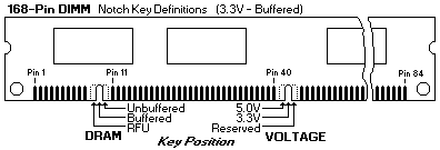
Keying Methodology
The (on top) figure shows the keying methodology employed on 8-byte DIMMs.
One key defines the device type and one key defines the voltage.
The voltage key provides a positive interlock so that DIMMs can only be plugged into a system with the proper supply
voltage, reducing potential damage to the module devices.
Unless the designer chooses the appropriate connector, the system will not work.
Note that an unbuffered 3.3V SDRAM DIMM and an unbuffered 3.3V DRAM DIMM can be plugged into the same memory slot.
I/O Interface Signal Usage
The 168 interface signals are divided into the following six groupings, discussed in the following subsections:
| Addressing | 16 |
|---|---|
| Data | 80 |
| Control | 21 |
| Serial PD | 5 |
| Power | 37 |
| Unused | 9 |
| Total: | 168 |
Addressing
The address interface consists of the following 16 input signals: A0 - A9, A10/AP, A11 - A13 and BA0 - BA1.
Signals A0 - A9 and A11 - A13 are row/column multiplexed addresses in a similar fashion to asynchronous DRAMs.
A10/AP is used as a row address at row address time but is used as the autoprecharge select during column address time.
As a minimum, A0 - A9 and A10/AP are used in all DIMM configurations.
Depending on DIMM/SDRAM configuration/density signals A11 - A13 may or may not be used.
If not used they are a NC (no connect) at the DIMM.
BA0 - BA1 are the SDRAM bank address signals. These signals must be valid at both row and column address time.
BA0 is always used. BA1 is used only in configurations with four bank SDRAMs. When not used BA1 is a NC at the DIMM.
Data
The data interface consists of the following 80 input/output signals:
DQ0 - DQ63 and CB0 - CB15. The DQ signals are the 64 data bits, the 16 CB signals are the check bits for ECC operation.
For x64 DIMMs the check bits are all unused and are NC at the DIMM.
For x72 DIMMs CB0 - CB7 are used and CB8 - CB15 are NC. For x80 DIMMs all check bits are used.
The control interface consists of the following 21 input signals:
S0 - S3, RAS, CAS, WE, CK0 - CK3, CKE0 - CKE1 and DQMB0 - DQMB7.
S0 - S3 are the chip select signals. For a 1 bank DIMM S0 and S2 are used and S1 and S3 are NC.
For a 2 bank DIMM all four signals are used.
CK0 is used in all configurations. In general, with a few possible exceptions, CK1 is used in all configurations containing greater than five SDRAMs, and CK2 - CK3 are used in configurations with greater than 10 SDRAMs. All unused clocks are terminated with a capacitor to approximate a load of four to five SDRAMs. For all clocks that drive less than four SDRAMs a padding capacitor is added such that the total clock net approximates a load of four to five SDRAMs.
In configurations where CKE1 is used, it is tied to a 10k ohm pull-up resistor, otherwise it is a NC.
Serial Presence Detect
The Serial PD interface consists of the following five signals:
SA0 - SA2, SCL and SDA. SA0 - SA2 are the address inputs, SCL is the clock input and SDA is the serial data input/output.
Power
The power interface consists of the following 37 signals: 17 supply voltage (VDD), 18 signal ground (Vss),
and two input reference voltage (VREF).
The VREF signals are intended to be used with future high speed electrical interfaces (such as SSTL).
For DIMMs using LVTTL these signals are NC at the DIMM.
Unused
There are 9 interface pins defined as either Don't Use (DU) or No Connect (NC). They are all treated as NC at the DIMM.
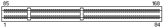
168-pin SDRAM DIMM PIN ASSIGNMENTS (Part 1 of 2)
Front Side (left side 1-42, right side 43-84) Back Side (left side 85-126, right side 127-168)
| Pin # | x64 Non-Parity |
x72 ECC |
x80 ECC |
Pin # | x64 Non-Parity |
x72 ECC |
x80 ECC |
|---|---|---|---|---|---|---|---|
| 1 | VSS | VSS | VSS | 85 | VSS | VSS | VSS |
| 2 | DQ0 | DQ0 | DQ0 | 86 | DQ32 | DQ32 | DQ32 |
| 3 | DQ1 | DQ1 | DQ1 | 87 | DQ33 | DQ33 | DQ33 |
| 4 | DQ2 | DQ2 | DQ2 | 88 | DQ34 | DQ34 | DQ34 |
| 5 | DQ3 | DQ3 | DQ3 | 89 | DQ35 | DQ35 | DQ35 |
| 6 | VDD | VDD | VDD | 90 | VDD | VDD | VDD |
| 7 | DQ4 | DQ4 | DQ4 | 91 | DQ36 | DQ36 | DQ36 |
| 8 | DQ5 | DQ5 | DQ5 | 92 | DQ37 | DQ37 | DQ37 |
| 9 | DQ6 | DQ6 | DQ6 | 93 | DQ38 | DQ38 | DQ38 |
| 10 | DQ7 | DQ7 | DQ7 | 94 | DQ39 | DQ39 | DQ39 |
| 11 | DQ8 | DQ8 | DQ8 | 95 | DQ40 | DQ40 | DQ40 |
| 12 | VSS | VSS | VSS | 96 | VSS | VSS | VSS |
| 13 | DQ9 | DQ9 | DQ9 | 97 | DQ41 | DQ41 | DQ41 |
| 14 | DQ10 | DQ10 | DQ10 | 98 | DQ42 | DQ42 | DQ42 |
| 15 | DQ11 | DQ11 | DQ11 | 99 | DQ43 | DQ43 | DQ43 |
| 16 | DQ12 | DQ12 | DQ12 | 100 | DQ44 | DQ44 | DQ44 |
| 17 | DQ13 | DQ13 | DQ13 | 101 | DQ45 | DQ45 | DQ45 |
| 18 | VDD | VDD | VDD | 102 | VDD | VDD | VDD |
| 19 | DQ14 | DQ14 | DQ14 | 103 | DQ46 | DQ46 | DQ46 |
| 20 | DQ15 | DQ15 | DQ15 | 104 | DQ47 | DQ47 | DQ47 |
| 21 | NC | CB0 | CB0 | 105 | NC | CB4 | CB4 |
| 22 | NC | CB1 | CB1 | 106 | NC | CB5 | CB5 |
| 23 | VSS | VSS | VSS | 107 | VSS | VSS | VSS |
| 24 | NC | NC | CB8 | 108 | NC | NC | CB12 |
| 25 | NC | NC | CB9 | 109 | NC | NC | CB13 |
| 26 | VDD | VDD | VDD | 110 | VDD | VDD | VDD |
| 27 | WE | WE | WE | 111 | CAS | CAS | CAS |
| 28 | DQMB0 | DQMB0 | DQMB0 | 112 | DQMB4 | DQMB4 | DQMB4 |
| 29 | DQMB1 | DQMB1 | DQMB1 | 113 | DQMB5 | DQMB5 | DQMB5 |
| 30 | S0 | S0 | S0 | 114 | S1 | S1 | S1 |
| 31 | DU | DU | DU | 115 | RAS | RAS | RAS |
| 32 | VSS | VSS | VSS | 116 | VSS | VSS | VSS |
| 33 | A0 | A0 | A0 | 117 | A1 | A1 | A1 |
| 34 | A2 | A2 | A2 | 118 | A3 | A3 | A3 |
| 35 | A4 | A4 | A4 | 119 | A5 | A5 | A5 |
| 36 | A6 | A6 | A6 | 120 | A7 | A7 | A7 |
| 37 | A8 | A8 | A8 | 121 | A9 | A9 | A9 |
| 38 | A10 /AP | A10 /AP | A10 /AP | 122 | BA0 | BA0 | BA0 |
| 39 | BA1 | BA1 | BA1 | 123 | A11 | A11 | A11 |
| 40 | VDD | VDD | VDD | 124 | VDD | VDD | VDD |
| 41 | VDD | VDD | VDD | 125 | CK1 | CK1 | CK1 |
| 42 | CK0 | CK0 | CK0 | 126 | A12 | A12 | A12 |
| 43 | VSS | VSS | VSS | 127 | VSS | VSS | VSS |
| 44 | DU | DU | DU | 128 | CKE0 | CKE0 | CKE0 |
| 45 | S2 | S2 | S2 | 129 | S3 | S3 | S3 |
| 46 | DQMB2 | DQMB2 | DQMB2 | 130 | DQMB6 | DQMB6 | DQMB6 |
| 47 | DQMB3 | DQMB3 | DQMB3 | 131 | DQMB7 | DQMB7 | DQMB7 |
| 48 | DU | DU | DU | 132 | A13 | A13 | A13 |
| 49 | VDD | VDD | VDD | 133 | VDD | VDD | VDD |
| 50 | NC | NC | CB10 | 134 | NC | NC | CB14 |
| 51 | NC | NC | CB11 | 135 | NC | NC | CB15 |
| 52 | NC | CB2 | CB2 | 136 | NC | CB6 | CB6 |
| 53 | NC | CB3 | CB3 | 137 | NC | CB7 | CB7 |
| 54 | VSS | VSS | VSS | 138 | VSS | VSS | VSS |
| 55 | DQ16 | DQ16 | DQ16 | 139 | DQ48 | DQ48 | DQ48 |
| 56 | DQ17 | DQ17 | DQ17 | 140 | DQ49 | DQ49 | DQ49 |
| 57 | DQ18 | DQ18 | DQ18 | 141 | DQ50 | DQ50 | DQ50 |
| 58 | DQ19 | DQ19 | DQ19 | 142 | DQ51 | DQ51 | DQ51 |
| 59 | VDD | VDD | VDD | 143 | VDD | VDD | VDD |
| 60 | DQ20 | DQ20 | DQ20 | 144 | DQ52 | DQ52 | DQ52 |
| 61 | NC | NC | NC | 145 | NC | NC | NC |
| 62 | VREF, NC | VREF, NC | VREF, NC | 146 | VREF, NC | VREF, NC | VREF, NC |
| 63 | CKE1 | CKE1 | CKE1 | 147 | NC | NC | NC |
| 64 | VSS | VSS | VSS | 148 | VSS | VSS | VSS |
| 65 | DQ21 | DQ21 | DQ21 | 149 | DQ53 | DQ53 | DQ53 |
| 66 | DQ22 | DQ22 | DQ22 | 150 | DQ54 | DQ54 | DQ54 |
| 67 | DQ23 | DQ23 | DQ23 | 151 | DQ55 | DQ55 | DQ55 |
| 68 | VSS | VSS | VSS | 152 | VSS | VSS | VSS |
| 69 | DQ24 | DQ24 | DQ24 | 153 | DQ56 | DQ56 | DQ56 |
| 70 | DQ25 | DQ25 | DQ25 | 154 | DQ57 | DQ57 | DQ57 |
| 71 | DQ26 | DQ26 | DQ26 | 155 | DQ58 | DQ58 | DQ58 |
| 72 | DQ27 | DQ27 | DQ27 | 156 | DQ59 | DQ59 | DQ59 |
| 73 | VDD | VDD | VDD | 157 | VDD | VDD | VDD |
| 74 | DQ28 | DQ28 | DQ28 | 158 | DQ60 | DQ60 | DQ60 |
| 75 | DQ29 | DQ29 | DQ29 | 159 | DQ61 | DQ61 | DQ61 |
| 76 | DQ30 | DQ30 | DQ30 | 160 | DQ62 | DQ62 | DQ62 |
| 77 | DQ31 | DQ31 | DQ31 | 161 | DQ63 | DQ63 | DQ63 |
| 78 | VSS | VSS | VSS | 162 | VSS | VSS | VSS |
| 79 | CK2 | CK2 | CK2 | 163 | CK3 | CK3 | CK3 |
| 80 | NC | NC | NC | 164 | NC | NC | NC |
| 81 | NC | NC | NC | 165 | SA0 | SA0 | SA0 |
| 82 | SDA | SDA | SDA | 166 | SA1 | SA1 | SA1 |
| 83 | SCL | SCL | SCL | 167 | SA2 | SA2 | SA2 |
| 84 | VDD | VDD | VDD | 168 | VDD | VDD | VDD |
NOTE: NC = No Connect DU = Don't Use
Pinout Differences: 168-pin Unbuffered DRAM vs Unbuffered SDRAM DIMM
| Pin # | DRAM DIMM | SDRAM DIMM |
|---|---|---|
| 28 | CAS0 | DQMB0 |
| 29 | CAS1 | DQMB1 |
| 30 | RAS0 | S0 |
| 31 | OE0 | DU |
| 39 | A12 | BA1 |
| 42 | DU | CK0 |
| 44 | OE2 | DU |
| 45 | RAS2 | S2 |
| 46 | CAS2 | DQMB2 |
| 47 | CAS3 | DQMB3 |
| 48 | WE2 | DU |
| 62 | DU | VREF, NC |
| 63 | NC | CKE1 |
| 79 | NC | CK2 |
| 111 | DU | CAS |
| 112 | CAS4 | DQMB4 |
| 113 | CAS5 | DQMB5 |
| 114 | RAS1 | S1 |
| 115 | DU | RAS |
| 122 | A11 | BA0 |
| 123 | A13 | A11 |
| 125 | DU | CK1 |
| 126 | DU | A12 |
| 128 | DU | CKE0 |
| 129 | RAS3 | S3 |
| 130 | CAS6 | DQMB6 |
| 131 | CAS7 | DQMB7 |
| 132 | DU | A13 |
| 146 | DU | VREF, NC |
| 163 | NC | CK3 |
NOTE: A10 on DRAM DIMM is also AP on SDRAM DIMM
Serial Presence Detect
The 168-pin Unbuffered SDRAM DIMM utilizes a serial EEPROM device for the Presence Detect function.
The serial EEPROM application notes describe the operations and data definitions in detail.
Presence Detect Information
| Module Configuration |
SDRAM Organization |
Option 1 # Bank Addr. |
RAS Addr |
CAS Addr. |
Option 2 # Bank Addr. |
RAS Addr. |
CAS Addr. |
|---|---|---|---|---|---|---|---|
| 1M x 64/72/80 | 1M x 16 | 1 | 11 | 8 | |||
| 2M x 64/72/80 | 1M x 16 | 1 | 11 | 8 | |||
| 2M x 64 | 2M x 32 | 2 | 11 | 8 | |||
| 2M x 64/72/80 | 2M x 8 | 1 | 11 | 9 | |||
| 4M x 64/72/80 | 2M x 8 | 1 | 11 | 9 | |||
| 4M x 64 | 2M x 32 | 2 | 11 | 8 | |||
| 4M x 64/72/80 | 4M x 4 | 1 | 11 | 10 | |||
| 4M x 64/72/80 | 4M x 16 | 2 | 12 | 8 | 1 | 13 | 8 |
| 8M x 64/72/80 | 4M x 16 | 2 | 12 | 8 | 1 | 13 | 8 |
| 8M x 64 | 8M x 32 | 2 | 13 | 8 | 2 | 12 | 9 |
| 8M x 64/72/80 | 8M x 8 | 2 | 12 | 9 | 1 | 13 | 9 |
| 16M x 64/72/80 | 8M x 8 | 2 | 12 | 9 | 1 | 13 | 9 |
| 16M x 64 | 8M x 32 | 2 | 13 | 8 | 2 | 12 | 9 |
| 16M x 64/72/80 | 16M x 4 | 2 | 12 | 10 | 1 | 13 | 10 |
| 16M x 64/72/80 | 16M x 16 | 2 | 13 | 9 | |||
| 32M x 64/72/80 | 16M x 16 | 2 | 13 | 9 | |||
| 32M x 64/72/80 | 32M x 8 | 2 | 13 | 10 | |||
| 64M x 64/72/80 | 32M x 8 | 2 | 13 | 10 | |||
| 64M x 64/72/80 | 64M x 4 | 2 | 13 | 11 |
NOTE: All options possible with SDRAM standards are shown
Allowable configurations: (Byte 11)
Functional Attributes:
Please see the LEGAL - Trademark notice.
Feel free - send a  for any BUG on this page found - Thank you.