|
|
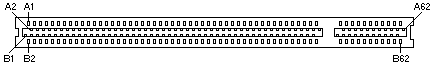 124-pin PCI-Connector
NOTE: 3.52Vdc is supplied through an opt. 5Vdc to 3.52 Vdc regulator.
| Pin | Signal | Pin | Signal |
|---|---|---|---|
| A1 | -TRST | B1 | -12 V |
| A2 | +12 V | B2 | TCK |
| A3 | TMS | B3 | Ground |
| A4 | TDI | B4 | TDO |
| A5 | +5 V | B5 | +5 V |
| A6 | -INTA | B6 | +5 V |
| A7 | -INTC | B7 | -INTB |
| A8 | +5 V | B8 | -INTD |
| A9 | Reserved | B9 | -PRSNT1 |
| A10 | +5 V (I/O) | B10 | Reserved |
| A11 | Reserved | B11 | -PRSNT2 |
| A12 | Ground | B12 | Ground |
| A13 | Ground | B13 | Ground |
| A14 | Reserved | B14 | Reserved |
| A15 | -RST | B15 | Ground |
| A16 | +5 V (I/O) | B16 | CLK |
| A17 | -GNT | B17 | Ground |
| A18 | Ground | B18 | -REQ |
| A19 | Reserved | B19 | +5 V (I/O) |
| A20 | AD(30) | B20 | AD(31) |
| A21 | +3.52 Vdc | B21 | AD(29) |
| A22 | AD(28) | B22 | Ground |
| A23 | AD(26) | B23 | AD(27) |
| A24 | Ground | B24 | AD(25) |
| A25 | AD(24) | B25 | +3.52 Vdc |
| A26 | IDSEL | B26 | -C/BE(3) |
| A27 | +3.52 Vdc | B27 | AD(23) |
| A28 | AD(22) | B28 | Ground |
| A29 | AD(20) | B29 | AD(21) |
| A30 | Ground | B30 | AD(19) |
| A31 | AD(18) | B31 | +3.52 Vdc |
| A32 | AD(16) | B32 | AD(17) |
| A33 | +3.52 Vdc | B33 | -C/BE(2) |
| A34 | -FRAME | B34 | Ground |
| A35 | Ground | B35 | -IRDY |
| A36 | -TRDY | B36 | +3.52 Vdc |
| A37 | Ground | B37 | -DEVSEL |
| A38 | -STOP | B38 | Ground |
| A39 | +3.52 Vdc | B39 | -LOCK |
| A40 | SDONE | B40 | -PERR |
| A41 | -SBO | B41 | +3.52 Vdc |
| A42 | Ground | B42 | -SERR |
| A43 | PAR | B43 | +3.52 Vdc |
| A44 | AD(15) | B44 | -C/BE(1) |
| A45 | +3.52 Vdc | B45 | AD(14) |
| A46 | AD(13) | B46 | Ground |
| A47 | AD(11) | B47 | AD(12) |
| A48 | Ground | B48 | AD(10) |
| A49 | AD(09) | B49 | Ground |
| A50 | Key | B50 | Key |
| A51 | Key | B51 | Key |
| A52 | C/BE(0) | B52 | AD(08) |
| A53 | +3.52 Vdc | B53 | AD(07) |
| A54 | AD(06) | B54 | +3.52 Vdc |
| A55 | AD(04) | B55 | AD(05) |
| A56 | Ground | B56 | AD(03) |
| A57 | AD(02) | B57 | Ground |
| A58 | AD(00) | B58 | AD(01) |
| A59 | +5 V (I/O) | B59 | +5 V (I/O) |
| A60 | -REQ64 | B60 | -ACK64 |
| A61 | +5 V | B61 | +5 V |
| A62 | +5 V | B62 | +5 V |
Please see the LEGAL - Trademark notice.
Feel free - send a  for any BUG on this page found - Thank you.