|
|
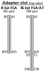
| Pin | Signal | Pin | Signal |
|---|---|---|---|
| B1 | Ground | A1 | -IOCHCK |
| B2 | RESET DRV | A2 | SD7 |
| B3 | +5 V | A3 | SD6 |
| B4 | IRQ2 | A4 | SD5 |
| B5 | -5 V | A5 | SD4 |
| B6 | DRQ2 | A6 | SD3 |
| B7 | -12 V | A7 | SD2 |
| B8 | -OWS | A8 | SD1 |
| B9 | +12 V | A9 | SD0 |
| B10 | Ground | A10 | IOCHRDY |
| B11 | -SMEMW | A11 | AEN |
| B12 | -SMEMR | A12 | SA19 |
| B13 | -IOW | A13 | SA18 |
| B14 | -IOR | A14 | SA17 |
| B15 | -DACK3 | A15 | SA16 |
| B16 | -DRQ3 | A16 | SA15 |
| B17 | -DACK1 | A17 | SA14 |
| B18 | -DRQ1 | A18 | SA13 |
| B19 | -REFRESH | A19 | SA12 |
| B20 | CLK | A20 | SA11 |
| B21 | IRQ7 | A21 | SA10 |
| B22 | IRQ6 | A22 | SA9 |
| B23 | IRQ5 | A23 | SA8 |
| B24 | IRQ4 | A24 | SA7 |
| B25 | IRQ3 | A25 | SA6 |
| B26 | -DACK2 | A26 | SA5 |
| B27 | TC | A27 | SA4 |
| B28 | BALE | A28 | SA3 |
| B29 | +5 V | A29 | SA2 |
| B30 | OSC | A30 | SA1 |
| B31 | Ground | A31 | SA0 |
| Pin | 16-Bit ext. | Pin | 16-Bit ext. |
| D1 | -MEMCS16 | C1 | -SBHE |
| D2 | -IOCS16 | C2 | LA23 |
| D3 | IRQ10 | C3 | LA22 |
| D4 | IRQ11 | C4 | LA21 |
| D5 | IRQ12 | C5 | LA20 |
| D6 | IRQ15 | C6 | LA19 |
| D7 | IRQ14 | C7 | LA18 |
| D8 | -DACK0 | C8 | LA17 |
| D9 | DRQ0 | C9 | -MEMR |
| D10 | -DACK5 | C10 | -MEMW |
| D11 | -DRQ5 | C11 | SD8 |
| D12 | -DACK6 | C12 | SD9 |
| D13 | -DRQ6 | C13 | SD10 |
| D14 | -DACK7 | C14 | SD11 |
| D15 | -DRQ7 | C15 | SD12 |
| D16 | +5 V | C16 | SD13 |
| D17 | -MASTER | C17 | SD14 |
| D18 | Ground | C18 | SD15 |
| Pin | VESA BUS | Pin | VESA BUS |
| F1 | Ground | E1 | -CMD |
| F2 | +5 V | E2 | -START |
| F3 | +5 V | E3 | EXRDY |
| F4 | N.U. | E4 | -EX32 |
| F5 | N.U. | E5 | Ground |
| F6 | Key | E6 | Key |
| F7 | N.U. | E7 | -EX16 |
| F8 | N.U. | E8 | -SLBURST |
| F9 | +12 V | E9 | -MSBURST |
| F10 | -M/IO | E10 | -W/R |
| F11 | -LOCK | E11 | Ground |
| F12 | Reserved | E12 | Reserved |
| F13 | Ground | E13 | Reserved |
| F14 | Reserved | E14 | Reserved |
| F15 | -BE3 | E15 | Ground |
| F16 | Key | E16 | Key |
| F17 | -BE2 | E17 | -BE1 |
| F18 | -BE0 | E18 | -LA31 |
| F19 | Ground | E19 | Ground |
| F20 | +5 V | E20 | -LA30 |
| F21 | -LA29 | E21 | -LA28 |
| F22 | Ground | E22 | -LA27 |
| F23 | -LA26 | E23 | -LA25 |
| F24 | -LA24 | E24 | Ground |
| F25 | Key | E25 | Key |
| F26 | LA16 | E26 | LA15 |
| F27 | LA14 | E27 | LA13 |
| F28 | +5 V | E28 | LA12 |
| F29 | +5 V | E29 | LA11 |
| F30 | Ground | E30 | Ground |
| F31 | LA10 | E31 | LA9 |
| H1 | LA8 | G1 | LA7 |
| H2 | LA6 | G2 | Ground |
| H3 | LA5 | G3 | LA4 |
| H4 | +5 V | G4 | LA3 |
| H5 | LA2 | G5 | Ground |
| H6 | Key | G6 | Key |
| H7 | SD16 | G7 | SD17 |
| H8 | SD18 | G8 | SD19 |
| H9 | Ground | G9 | SD20 |
| H10 | SD21 | G10 | SD22 |
| H11 | SD23 | G11 | Ground |
| H12 | SD24 | G12 | SD25 |
| H13 | Ground | G13 | SD26 |
| H14 | SD27 | G14 | SD28 |
| H15 | Key | G15 | Key |
| H16 | SD29 | G16 | Ground |
| H17 | +5 V | G17 | SD30 |
| H18 | +5 V | G18 | SD31 |
| H19 | -MAKx | G19 | -MREQx |
Please see the LEGAL - Trademark notice.
Feel free - send a  for any BUG on this page found - Thank you.