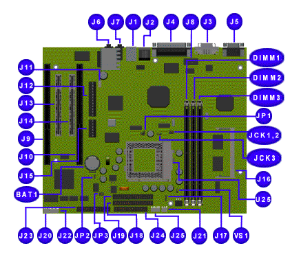
5242 System Board
Connector information
| Function | Description | Reference Designator |
| Keyboard | Miniature 6-pin | ˝J1 |
| Mouse | Miniature 6-pin | ˝J1 |
| Parallel port | DSUB 25-pin | J4 |
| Serial port | DSUB 15-pin | J8 |
| Ethernet connector | RJ45 | J2 |
| Flat panel monitor connector | 20-pin DFPP | J3 |
| Video | 15-pin VGA | J5 |
| Microphone in | Mini stereo | ˝J7 |
| Speaker out | Mini stereo | ˝J6 |
| Line out | Mini stereo | ˝J7 |
| Line in | Mini stereo | ˝J6 |
| DIMM sockets | 168-pin DIMM | DIMM 1 - 3 |
| SODIMM socket | 144-pin SODIMM | J16 |
| Socket 7 | 321-pin PGA | U25 |
| Socket 7 clock multiplier | 6-pin header | JP1 |
| SDRAM clock source | 3-pin header | JCK1 |
| CPU bus clock select | 3-pin header | JCK2 |
| CPU bus speed select | 2-pin header | JCK3 |
| Battery socket | Battery holder | BAT1 |
| Power supply | 6- and 12-pin ATPWR headers | J15, J12 |
| PCI slots | 32-bit PCI connector | J13, J14 |
| ISA slots | 16-bit ISA connector | J9, J10 |
| CD-ROM audio | 4-pin header, key 2 | J11 |
| IDE drives | 40-pin headers, key 20 | J18, J19 |
| Diskette drive | 34-pin header | J24 |
| Headphone board | 5-pin 2mm connector | J22 |
| Internal speakers | 2-pin header | J20, J21 |
| Game | DSUB 15-pin | J23 |
| CPU core voltage select | 6-pin header | JP3 |
| Second fan | 4-pin header, key 2 | J17 |
| CPU pin U33 voltage select | 3-pin header | VS1 |
| CMOS clear | 3-pin header | JP2 |
| Button board | 5-pin header | J25 |
JP1 (CPU clock multiplier) |
|||||||||
| CPU clock speed | 100 MHz bus | 200 | 250 | 300 | 350 | 400 | 450 | 500 | 550 |
| 95 MHz bus | 190 | 238 | 285 | 333 | 380 | 428 | 475 | 523 | |
| pins 1-2 | on | on | off | off | on | on | off | off | |
| pins 3-4 | off | on | on | off | off | on | on | off | |
| pins 5-6 | off | off | off | off | on | on | on | on | |
JCK3 (CPU bus speed select) |
||
| CPU bus speed (MHz) | 95 | 100 |
| Pins 1-2 | on | off |
* The factory default settings of the following jumpers are marked with an asterisk (*). These settings will not normally need to be adjusted.
JCK1 (SDRAM clock source) |
||
| CMOS state | CPU clock* | AGP clock |
| Jumper position | pins 1-2 | pins 2-3 |
JCK2 (CPU bus clock select) |
||
| CMOS state | 66 MHz bus | 95 or 100 MHz bus* |
| Jumper position | pins 1-2 | pins 2-3 |
VS1 (CPU pin U33 voltage select) |
||
| U33 voltage | 3.3 V* | 3.45 V |
| Jumper position | pins 1-2 | pins 2-3 |
JP3 (CPU core voltage select) |
||||||||
| VCC2H/L# low | 2.0 | 2.1 | 2.2* | 2.3± | 2.4 | 2.5 | 2.6 | 2.7 |
| VCC2H/L# high | 2.8 | 2.9 | 3.0 | 3.1 | 3.2 | 3.3 | 3.4 | 3.5 |
| pins 1-2 | off | on | off | on | off | on | off | on |
| pins 3-4 | off | off | on | on | off | off | on | on |
| pins 5-6 | off | off | off | off | on | on | on | on |
| ± These settings must be used for the 450MHz K6-2 processor. | ||||||||